
12th ki History ki best file with decoration YouTube
Double-click on the 'pro' (project) file. The main KiCad window will appear. This window is the launch pad for the other KiCad apps, like Eeschema (the schematic editor) and Pcbnew (the layout editor). You can see the main KiCad window in Figure 5.2. Figure 5.2: The main KiCad window.

School Project Front Page Design 187 Picture Density Gambaran
Product Designer and UX Architect with a natural instinct for growth and navigating ambiguity. I've led design and built highly performing products for several Fortune 500 companies, early-stage startups, and award-winning agencies.
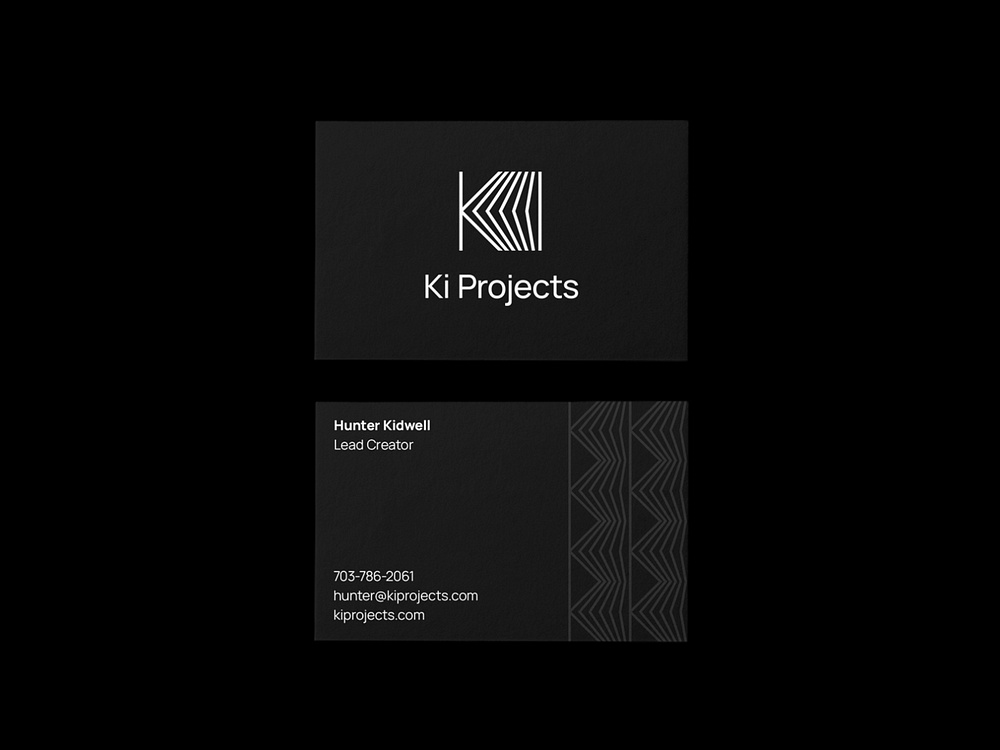
Ki Projects logo design by Milos Bojkovic on Dribbble
Donating to KiCad via The Linux Foundation provides funds for project development and the developers behind it. Donations are accepted via credit card and purchase order (US$ only). The Linux Foundation is a 501(c)(6) non-profit organization in the US. Donate via TLF
Saari ki design ki setting by nilesh wankhade YouTube
KiCad EDA A Cross Platform and Open Source Electronics Design Automation Suite Documentation Download See what's new Schematic Capture KiCad's Schematic Editor supports everything from the most basic schematic to a complex hierarchical design with hundreds of sheets.

Buy Devin Townsend Project Ki CD Sanity Online
KiCad is an open-source software suite for creating electronic circuit schematics, printed circuit boards (PCBs), and associated part descriptions. KiCad supports an integrated design workflow in which a schematic and corresponding PCB are designed together, as well as standalone workflows for special uses.

KI Dexigner
Careers kidesign.io/careers Media Inquiries Leave a message Ready to bring your digital vision to life? Contact Ki Design today and collaborate with our team of experts to create something truly exceptional.

VDA Leitinitiative launches another AI project KI Familie now complete
Stay organized with the MEL Design Wizard! Organize and define your data collection tools in 3 easy steps: 1 - Identify the sources you need to collect data from (e.g. groups of project.

KIArchitekt DalleWettbewerber Midjourney die Wolkenkratzer der Zukunft
These are some KiCad designed projects that have been made by users. If you want to be featured along the other showcases on this page please submit a merge request on GitLab if you meet the contributing guidelines for requirements on adding a project! «« « 1 2 3 4 5 » »» A64-OLinuXino Olimex

Ki Projects logo design by Milos Bojkovic on Dribbble
Roberta MK Fox, AIA, ASLA is the founder, owner, and lead designer of Catalyst Design PLLC. She has over 20 years experience practicing architecture, landscape architecture, and urban design for both private and public-sector projects with a special focus on strategic planning, project delivery, transportation architecture, and the people-centered spaces around them.

Ghar Ka Design YouTube
About Press Copyright Contact us Creators Advertise Developers Terms Privacy Policy & Safety How YouTube works Test new features NFL Sunday Ticket Press Copyright.

How To Decorate First Page Of Project File Easy / Project file cover decoration/file decoration
Let's go over each of the steps needed to create a project design. Step 1. Define project goals. In the first step, define your project goals. To begin, lead an initial ideation meeting where you document the general project timeline and deliverables. To start, consider the needs of the project and stakeholders.

मकान की डिजाइन बनाने का आसान तरीका mountain ki ki design Makan ki ki design YouTube
A project design is a blueprint that transforms your project vision into achievable goals. It offers a structured pathway for teams to follow. By defining your goals, establishing outcomes, understanding risks and visualizations, preparing contingency plans, making a budget, and developing monitoring procedures, ensure your project begins and.
Jhumar Banane Ki Design Bataen
The default soldermask clearance is 0.1mm per side in Eagle. In KiCad's Pcbnew, open the ZOPT220x Breakout and click on Dimensions -> Pads Mask Clearance. KiCad's solder mask clearance has a default of 0.2mm per side. We recommend you change this value to 0.1mm. Most fab houses will use 0.1mm as their default as well.

Best Mehndi Designs For Different Occasions Diwali special Unique Mehndi Designs
2. Starting a New Project. When you open up KiCad, you'll see the window shown in Image 2.1. From here, you can open or create new projects. To create a new project, click on the File menu and select New -> Project. Choose where you want to save your project and type in a name for it. Then click on the Save button. Image 2.1 The main KiCad window

AGIKgqMvBiGoxZnhjmhTv7hM2hboV2so9PVfcVuS9mrU=s900ckc0x00ffffffnorj
Get notified about new Project Design Coordinator jobs in Raleigh, NC. Sign in to create job alert Similar Searches Supervisor jobs 1,307,149 open jobs Specialist jobs.

Mehandi ki design 🙏 YouTube
TOKYO, January 9, 2024-Sony Corporation announced development of an immersive spatial content creation system, which includes an XR head-mounted display equipped with high-quality 4K OLED Microdisplays *2 and video see-through function, and a pair of controllers optimized for intuitive interaction with 3D objects and precise pointing. The system is aimed at supporting creators in sophisticated.